Micron Technology’s 3D NAND Roadmap for 2017
Micron Technology (MU) plans to spend ~$1.8 billion in capex on ramping up the 64-tier 3D NAND and developing the third-generation 3D NAND.
March 27 2017, Updated 10:36 a.m. ET

NAND product mix
Micron Technology (MU) is rebalancing its DRAM (dynamic random access memory) product mix to focus on its Mobile, Server, and Embedded segments. On the NAND side, the company has been mainly focusing on the Storage and Mobile segments and less on the Consumer segment. However, it did not achieve much success with planar NAND due to its high cost.
Micron Technology has moved to 3D technology and is expected to maintain the same mix. Its 3D NAND has been qualified for storage applications. Its 3D TLC (triple-level cell) in the MTP (multi-time programmable) is currently in the qualification process for mobile applications.
Micron’s 32-tier 3D NAND
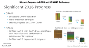
In 2016, Micron Technology (MU) transitioned from 16nm (nanometer) planar NAND to 32-tier 3D NAND and achieved mature yields. In 2015, Micron projected that it could achieve 25% cost improvement from this transition. However, the actual figure was even better, with 30% cost improvement.
For the first time, the company achieved similar yields on both 3D NAND TLC and MLC (multi-level cell). Moreover, the performance of TLC is better on 3D NAND than the performance of MLC is on planar NAND.
Micron Technology claims that its 3D NAND beats its planar NAND in terms of performance, as well as the 3D NAND of its competitors. It stated that its 32-tier node is almost equivalent to competitors’ 48-tier nodes with just a slight difference in bit density. This performance is a result of its 3D NAND architecture CMOS[1. complementary metal-oxide-semiconductor] Under the Array.
Micron Technology claims that its 3D NAND not only beats its planar NAND but also the 3D NAND of its competitors. It stated that its 32-tier node is almost equivalent to competitors’ 48-tier nodes with just a slight difference in bit density. This performance is a result of its 3D NAND architecture CMOS (complementary metal-oxide-semiconductor) Under the Array.
Micron’s spending in 3D NAND
Micron Technology (MU) plans to spend ~$1.8 billion in capex on ramping up the 64-tier 3D NAND and developing the third-generation 3D NAND. The company expects the transition to 64-tier 3D NAND to bring 30% cost improvement and 60% growth in 3D NAND output by the end of 2017.
To achieve 60% growth in NAND bit output, Micron Technology would have to reach the yield it achieved from 32-tier nodes from its 64-tier technology as early as the summer of 2017. Moreover, the planar NAND output must decrease to zero.
The company has been expanding its Singapore (EWS) facility to build 3D NAND, but it didn’t give details about the technology. There is a possibility that it may be ramping 64-tier 3D NAND there, and it may bring the full capacity of 140,000 wafers per month online by the summer of 2017.
Micron claims that its 64-tier technology has more than 25% more die per wafer relative to any competitor’s 64-tier technology. Its 64-tier technology has a die size of 59 square millimeters, making it the world’s smallest 256-gigabit die. Samsung (SSNLF), Toshiba (TOSBF)/Western Digital (WDC), and SK Hynix are also developing 3D NAND using different architectures.
Next, we’ll look at Micron Technology’s plans for QLC (quad-level cell).
