Xilinx Prepares Gears up with ARM’s IP
Xilinx (XLNX) is moving ahead of Intel (INTC), not only in FPGA (field programmable gate array) adoption but also in technology node.
Dec. 23 2016, Updated 10:36 a.m. ET

Xilinx with ARM and TSMC
Xilinx (XLNX) is moving ahead of Intel (INTC), not only in FPGA (field programmable gate array) adoption but also in the technology node. Xilinx is already a year ahead of Intel with its 16 nm (nanometer) FPGA and is now preparing for 7 nm chips.
Xilinx is extending its partnership with ARM Holdings (ARMH) beyond 28 nm, 20 nm, and 16 nm. Xilinx has become the first company to license ARM’s Artisan Physical IP (intellectual property) platform for 7 nm. Specifically, Xilinx plans to use this IP to design its next FPGA on Taiwan-based (EWT) TSMC’s (TSM) 7 nm FinFET (Fin Field Effect Transistor) process technology.
Xilinx’s move to 7 nm
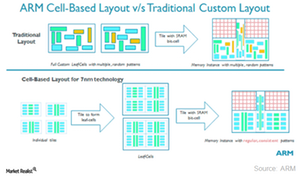
The product manager of ARM’s physical design group, Ron Moore, recently explained the layout of the 7 nm design built on the Artisan platform. The 7 nm design faced three major challenges: variation in the process as chip sizes shrink, difficulty in routing designs, and the functioning of electrical properties like electromigration.
ARM addressed these challenges with a cell-based layout that brings consistency in a pattern while reducing variation in the process. ARM filled the empty spaces and stacked all components in the first two metal layers, thereby improving routing and leaving the upper layers completely for SoC (system-on-chip) designer to customize the chip.
The earlier chip designs only used the front end-of-line device. However, the ARM Artisan platform uses both the front and back end-of-line devices to provide enhanced performances. This should help the 7 nm chip differentiate itself from the 14 nm chip.
ARM offers semi-custom chip designs
ARM offers specialized libraries and tools to use these standard chip designs to create chips for a variety of processes such as FPGA, mobile SoC, and server processors. In this way, ARM provides semi-custom chips without putting too many man hours into designing full custom chips.
One of the key aspects of the shrinking node is an improvement in power efficiency. As the node shrinks the issue of powering the various areas of the SoC becomes complex. ARM has therefore built a Power Grid Architect that has the knowledge of Artisan logic libraries. This accelerates the tedious task of developing correct-by-construction power grids from weeks to hours.
TSMC is currently developing the 7 nm node and plans to ramp production of the same sometime in 2018. Xilinx may start the initial testing of its 7 nm FPGA with a few partners in calendar 1H17.
Meanwhile, Intel has been developing its 10 nm node, which it plans to ramp up production for in late 2017.
