TSMC Has Accelerated Advanced Technology Development
TSMC is currently ramping up production of its 16nm technology. It expects to complete it by the end of fiscal 2Q16.
April 21 2016, Updated 9:07 a.m. ET

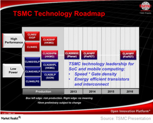
TSMC’s technology roadmap
In the previous part of the series, we saw that Taiwan Semiconductor Manufacturing Company (or TSMC) (TSM) has been ramping up its 16/20nm (nanometer) technology in order to secure more orders. The company has been shifting its production according to the market trend. Let’s look now at the company’s technology roadmap and investments in plants and machinery.
Investing in 16nm and beyond
TSMC is currently ramping up production of its 16nm technology. It expects to complete it by the end of fiscal 2Q16. It plans to start ramping up its 10nm technology at two of its 12-inch giga-fabs (fabrication facilities) with an aim to have a capacity of 200,000 wafers per quarter by the second half of 2016. Intel (INTC) is also working on 10nm technology but has delayed it to 2017. The 10nm would attract mobile customers.
TSMC also plans to develop 7nm technology by 1Q17, with production ramp-up planned in the first half of 2018. The 7nm is just an advancement of the 10nm with more than 95% common tools. The 7nm would be more than 60% denser and 30%–40% more power efficient than 10nm. It would attract manufacturers of GPUs (graphic processing units), FPGAs (field programmable gate arrays), and other consumer product applications.
Investing in plant and machinery
To support the aggressive technology ramp-up, TSMC has placed orders for machinery equipment at various SME (semiconductor manufacturing equipment) suppliers. This includes a $16.7 million order from Applied Materials (AMAT) and a $37 million order from KLA-Tencor (KLAC).
TSMC and the city government of Nanjing, China, have signed an agreement to spend $3 billion on a 12-inch wafer fabrication facility in China. Given the tension between China and Taiwan over protection of intellectual property, the facility would be wholly owned by TSMC. It would have a capacity to manufacture 20,000 12-inch wafers a month. TSMC is expected to begin production in the second half of 2018. The company also plans to build a design service center inside the facility.
Acquiring third-party patents
TSMC has also signed a patent licensing and sales agreement with Canada’s (EWC) NPE WiLAN. As part of the deal, TSMC can use NPE WiLAN’s semiconductor process technology patents. It can also use Polaris, a portfolio of more than 7,000 former Qimonda patents that NPE acquired from Infineon in June 2015. TSMC also acquires third-party patents by investing in start-ups through its venture capital arm TSMC Partners.
In the next part of the series, we’ll look at the company’s cash position to fund these developments.
