Behind Intel’s Foundry Business
Intel’s process leadership is seemingly unbeatable. Its upcoming 10nm (nanometer) node will contain double the number of transistors compared to Samsung’s and TSMC’s 10nm nodes.
April 27 2017, Updated 10:38 a.m. ET

Intel an unrivaled process leader
Intel’s (INTC) process leadership is seemingly unbeatable. Its upcoming 10nm (nanometer) node will contain double the number of transistors compared to Samsung’s (SSNLF) and TSMC’s (TSM) 10nm nodes.
Intel claims that the transistor density in its 10nm nodes will convert into a CPU (central processing unit) that has 25% better performance and 45% lower power consumption than its 14nm KabyLake.
Moreover, its 10nm node should give it a 30% cost advantage over Advanced Micro Devices (AMD), which is building its CPUs on GF’s (GlobalFoundries) 14nm node.
Intel plans to optimize its 10nm node over the next three years by introducing enhancements such as the 10+ and 10++. With every process refinement, the node’s performance and power efficiency are expected to improve 15% and 30%, respectively.
Intel fab utilization falls
However, Intel wants to cash out on its process leadership, as its fabrication facilities, or fabs, aren’t being utilized to their full capacities. The PC (personal computer) and server markets require a large number of chips, and because of this, Intel has built capacity and developed advanced processes to improve yield and performance.
However, the PC market has stagnated, and demand for server processors has slowed, adversely impacting Intel’s revenue and fab utilization. The fixed cost of maintaining a fab and the rising cost of developing new process nodes is increasing the company’s cost of production. Hence, Intel is entering the foundry business to improve its fab utilization and get a better return on its investments.
Intel’s foundry model
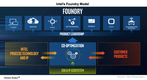
At its Technology Manufacturing Day in March 2017, Intel’s president of manufacturing, operations, and sales, Stacy Smith, explained the foundry opportunity. Smith stated that the total addressable market of the foundry was $53 billion in 2016, of which $23 billion was for advanced nodes of 28nm and smaller. Only a few foundries, namely TSMC, Samsung, GF, and IBM (IBM), have advanced nodes of 22nm or smaller.
Intel’s process nodes are more advanced, giving it a technological advantage over its peers. Intel has partnered with ARM to manufacture ARM’s chips. This move should help it tap into companies that use ARM’s chip design such as Qualcomm, Lenovo, and Apple (AAPL). Intel’s key target is to secure a manufacturing contract from Apple that outsources the production of its A10 processors used in iPhones to TSMC.
Intel can optimize its process nodes and its customers’ chip architectures to make its foundries flexible for manufacturing all types of chips. It can use this flexible capacity to manufacture its own products at no additional cost.
Intel is also looking to optimize various nodes to create advanced chip designs. Because it’s becoming increasingly difficult and costly to shrink nodes, Intel has adopted a heterogeneous design approach to manufacturing new chips. We’ll take a closer look at this approach in the next article.
