Advanced Nodes Increase TSMC’s Capital Expenditure
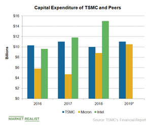
In the first three quarters of 2018, TSMC spent $6.7 billion in capital expenditure and is expected to spend $3.3 billion in the fourth quarter as it ramps up 7-nm production.
Nov. 20 2020, Updated 3:40 p.m. ET

TSMC increases its 2019 capital expenditure  
In the previous part of the series, we saw that TSMC (TSM) has been increasing its R&D (research and development) efforts on advanced 7-nm+ (nanometer) and 5-nm process nodes. These nodes would use capital-intensive EUV (extreme ultra violet) technology, which would mean an increase in the foundry’s capital expenditure.
In the first three quarters of 2018, TSMC spent $6.7 billion in capital expenditure and is expected to spend $3.3 billion in the fourth quarter as it ramps up 7-nm production. For 2019, it has set aside $10 billion to $12 billion for capital expenditure, up from $10 billion in 2018. Even Micron (MU) increased its capital spending from $5.25 billion in fiscal 2017 to $8.2 billion in fiscal 2018 to $10.5 billion in fiscal 2019.
Advanced nodes
TSMC would use the capital expenditure to upgrade to 7-nm, 7-nm+, and 5-nm nodes. An EET Asia article from October 5 stated that the foundry has already taped out its first customer 7-nm+ node. Tape-out is the final stage of chip design before it is sent for production. It expects to start risk production on the 5-nm node as early as April 2019 and move to volume production by the third quarter of 2020.
In the 7-nm+ node, TSMC plans to use EUV technology on up to four layers and increase its usage on up to 14 layers in the 5-nm node. Samsung (SSNLF) and Intel (INTC) also plan to use EUV technology for their 7-nm nodes. The growing adoption of this technology helped EUV machine supplier ASML Holding (ASML) report strong third-quarter earnings and stronger-than-expected fourth quarter revenue guidance.
As advanced nodes become more complex, lengthy, and capital intensive, TSMC is expanding its fabrication facilities to build advanced packaging to optimize capacity planning and enhance ROIC (return on invested capital).
Advanced packaging
According to a Fudzilla article, TSMC is looking to build a new advanced packaging plant in Taiwan to expand its backend wafer processing business. It is looking to offer system-on-integrated-chips and wafer-on-wafer packaging services to strengthen its competitiveness. This capital spending could improve TSMC’s profit margin, thereby improving its ROIC.
Check out all the data we have added to our quote pages. Now you can get a valuation snapshot, earnings and revenue estimates, and historical data as well as dividend info. Take a look!
