Applied Materials: A detailed business overview
According to Gartner, Applied Materials is the world’s largest maker of semiconductor equipment by revenues.
Jan. 14 2015, Updated 12:41 p.m. ET

Business overview
Applied Materials (AMAT) provides manufacturing equipment, software, and services to the global semiconductor, flat panel liquid crystal display (or LCD), solar photovoltaic (or PV), and related industries. Its core customers include manufacturers of semiconductor wafers and chips, flat panel LCD and other displays, solar PV cells and modules, and other electronic devices. Founded in 1967, Applied Materials announced the acquisition of Tokyo Electron in 2013. It later announced that both firms plan to merge, forming another company called Eteris, which we will explore later in this series.
Semiconductor manufacturing market leader
According to Gartner, Applied Materials is the world’s largest maker of semiconductor equipment by revenues, followed by ASML Holding NV (ASML), Lam Research (LRCX), and Tokyo Electron. Applied Materials and Tokyo Electron reported fiscal 2013 revenues of $5.46 billion and $3.06 billion, respectively. In 2013, Applied Materials and Tokyo Electron commanded a market share of 16.2% and 9.1%, respectively.
Reportable segments
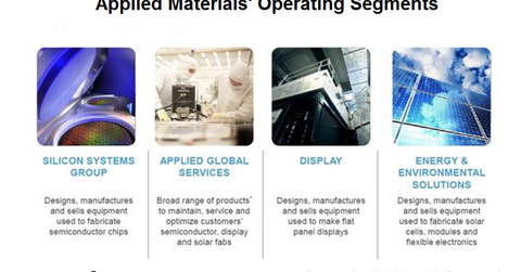
The company primarily generates its revenue from the following reportable segments, as shown in the chart above:
- Silicon Systems Group
- Applied Global Services
- Display
- Energy and Environmental Solutions
- End markets and customers
Taiwan Semiconductor Manufacturing (TSM) and Samsung Electronics (SSNLF) are Applied Materials’s major customers, contributing 21% and 12%, respectively, toward fiscal 2014’s overall revenues. Intel (INTC) is also a key customer of both Applied Materials and Tokyo Electron. Geographically, Asia Pacific, the United States, and Europe contributed 71%, 22%, and 7%, respectively, to the overall revenues in fiscal 2014.
